Detector configurations
Below some general aspects are mentioned regarding detector construction which may help you choosing the right detector for your application.
Detector configurations
Below some general aspects are mentioned regarding detector construction which may help you choosing the right detector for your application.
Scintillation crystals without photomultiplier tubes
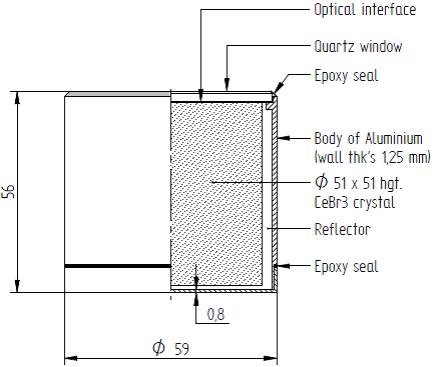
A scintillation crystal can be supplied to fit a specifically designed instrument of a user. Often, the scintillation crystal is supplied mounted in a hermetically sealed metal container with an optical window to protect the crystal from hydration or from other environmental influences. In case of non-hygroscopic crystals this requirement is less stringent.
Because of statistics, it is always desirable to detect as much light as possible from a scintillation event in the light detection device. For this purpose, the scintillation crystal is covered on all sides, except the read-out side, with reflective material. This can be e.g. special white reflective materials like TYVEK, Teflon or reflective powder such as Al2O3. The surfaces in contact with the reflector can be optically polished or ground. The scintillation light is transmitted through a glass or quartz window to be optically coupled to the light detector.
Depending on the shape of the scintillation crystal, a certain surface treatment is required to obtain a large light output and a good uniformity. Both are important to achieve a good energy resolution. The optimization of scintillation crystal surfaces is based on experience with the material and not always obvious. SCIONIX will provide the optimum surface treatment of the crystal for your specific application.
Optical coupling to the PMT can be achieved by using optical grease or a special optically transparent glue. Below, an example of the general construction of a canned scintillation crystal is shown. Flexible optical coupling allows for different expansion coefficients between materials.
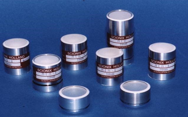
Standard C-style scintillation assembly
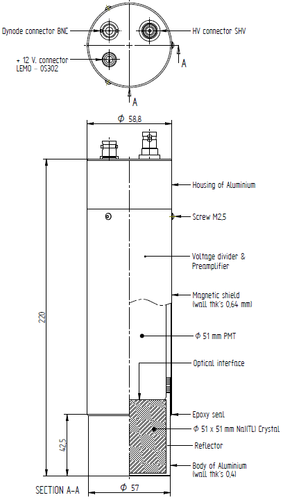
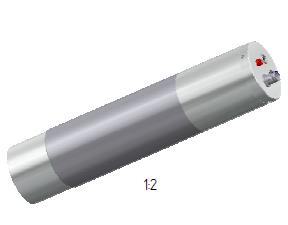
Scintillation crystals with photomultiplier tubes
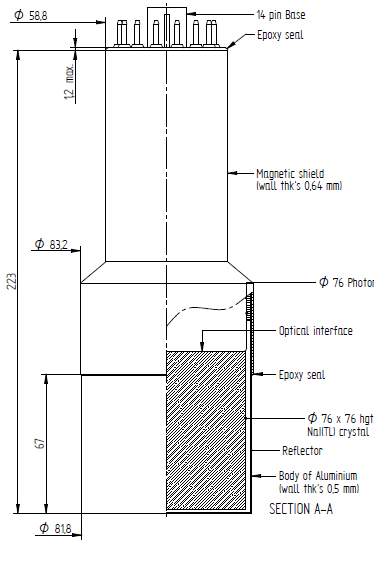
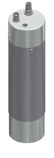
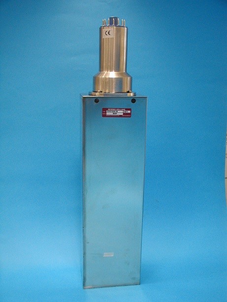
The most frequently used scintillation detector consists of a scintillation material integrally coupled to a Photomultiplier Tube (PMT). The scintillation crystal is mounted in a metal housing with μ-metal shielding against the influence of magnetic fields. For conditions where strong fields are expected, this shield can be increased in thickness for additional protection.
.
 |
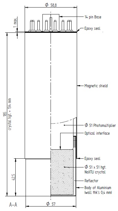 |
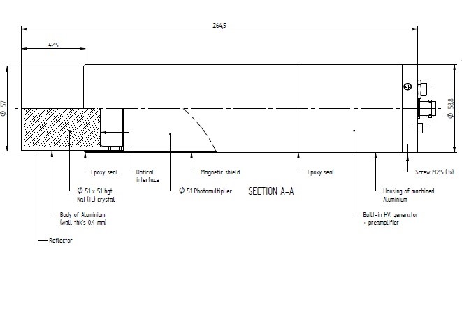
Standard 51B51/2M scintillation detector
.
 |
 |
.
Standard 76B76 / 3M scintillation detector
.
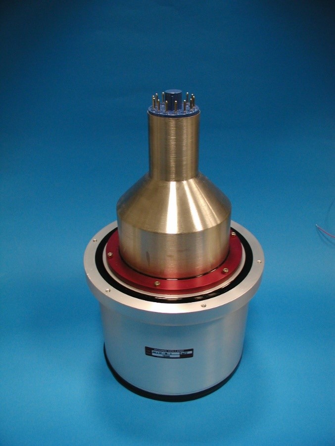
Standard scintillation detectors read out with PMTs can be provided with either an external so called “plug-on” Voltage Divider (VD) for the PMT or with a built-in one. In the first case, the detector itself ends in a 12, 14, or 20 pins connector that should be plugged into the socket of the VD or so called digital base”. This allows quick exchange of detectors and electronics but it makes the detector considerably longer (about 5 cm).
In addition to a voltage Divider it is possible to incorporate a preamplifier / line driver into the detector that converts the high impedance output signal of the PM to a 50 Ohms output signal that can drive over 100 m of cable.
51×51 mm scintillation detectors with built-in line driver
.
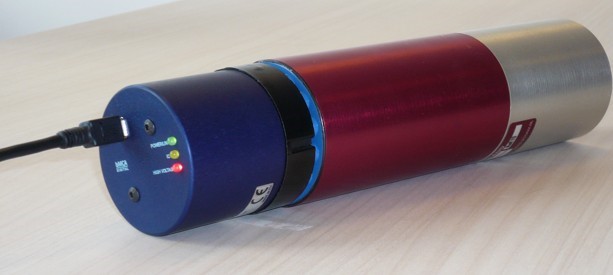
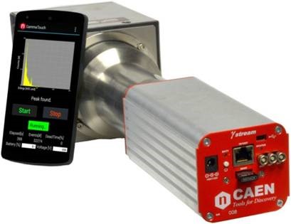
A ”digital base” is a piece of electronics that is connected to a scintillation detector with 14 or 20 pins and which produces the required high voltage, processes the signals and digitizes them. It is connected via a USB, Ethernet port or sometimes via a Bluetooth connection to a computer or cell phone.
Click image (zoom)
Example of digital bases
.
Besides built-in Voltage Dividers /preamplifiers), it is also possible to integrate high voltage generators (fed with +5 or +12 V) into the assembly or spectroscopic amplifiers and counters. Both can be fed with external voltages via a power connector or a USB connector.
 |
 |
For more details regarding detector electronics we refer the respective section.
Photodiode detectors
The advantages and limitations of these instruments were already discussed in the section about light detectors In general. The required size of the scintillation crystal determines the possibility to use this readout technique. Small crystals perform best with good energy resolution and noise levels around 50 keV or slightly less. For medical applications these devices are well suited for measurement of 140 keV gamma-rays.
Photodiode detectors are also widely used for heavy ion detection in combination with thin Si detectors for E / ΔE measurements applied to particle identification. Compact size, good energy resolution and immunity to magnetic fields are pro’s.
.
.
.
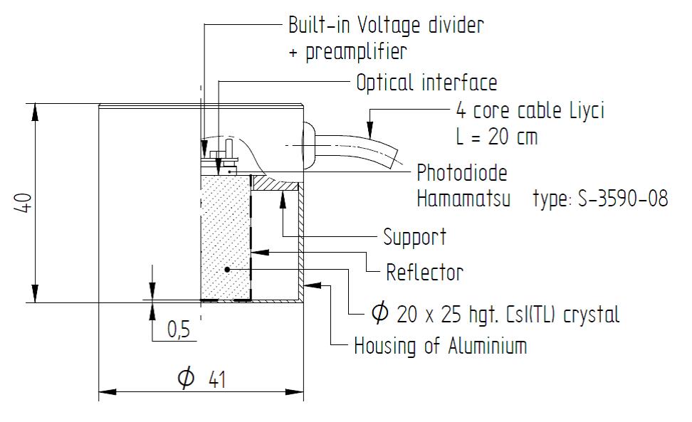
20×25 mm CsI(Tl) PIN Photodiode detector with built-in preamplifier
A totally different application is the measurement of high intensity X-ray beams. In this case, the photodiode is used in DC current mode (no pulse height discrimination). Longer wavelength emitting scintillation crystals like CsI(Tl), CdWO4 or special ceramic scintillators are sometimes used in arrays coupled to photodiodes. Advantages are the good signal reproducibility, the absence of gain drift and the compact size.
.
.
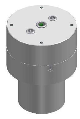
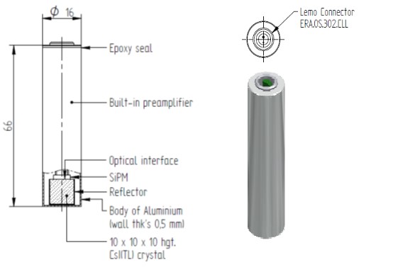
Silicon Photomultiplier (SiPm) readout
SiPm readout can result in compact mechanically robust scintillation detectors especially when rugged scintillators like CsI(Tl) are used. The required bias voltage that SiPms need (often 25-30 V) can be generated using built-in charge pumps operating at low voltages and consuming tens of mW. The raw SiPm signal, differentiated to increase is speed or a preamplified signal is fed out. The intrinsic large gain drift of SiPms (> -1% per degree C) can be overcome to a large extent by the built-in temperature compensation of the bias generator.
Usually only a fraction (20-30 %) of the total scintillator surface is covered with SiPm area to limit the cost of the sensor. This is sufficient for most applications. When more area of the scintillator is covered it increases the signal but also the noise. The optimum choice depends on the sensor requirements in terms of time- , energy resolution and noise.

38×38 mm CeBr3 scintillator with SiPm readout
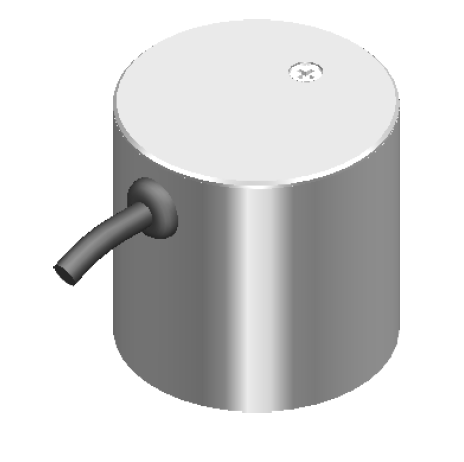
Miniature CsI(Tl) SiPm detector with built-in power supply
Detector entrance windows
The density and thickness of the detector entrance window determine the transmission of the radiation. For high energy gamma-rays say > 300 keV, the absorption of a mm or so entrance window can be neglected and the choice for a window is dictated by practical considerations.
For lower energy X-rays this choice is more critical. Below, the transmission of a range of standard detector windows is presented from which you can determine the optimum window for your application. The thinnest Aluminum window normally used has a thickness of 25 -30 μm. This window can be used down to 10 keV X-ray energy. Below this energy, 0.2 or 0.3 mm thick Beryllium is required. The advantage of a Be window above a thin aluminum one is that is it less fragile.
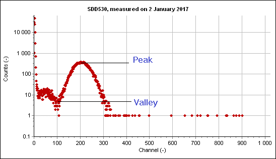
Typical 5.9 keV 55Fe energy spectrum measured with a NaI(Tl)
scintilation detector showing a typical nergy resolution
< 40 % FWHM and peask-to valley ration > 45
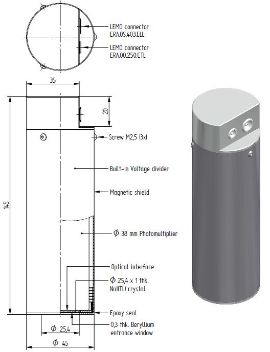
NaI(Tl) X-ray detector with built-in Voltage Divider
For the detection of alpha particles or low energy electrons (beta particles), a thin aluminized (light tight) mylar window is used. Mylar windows however can only be applied for non-hygroscopic scintillation materials. Standard thickness is 2,4, 6 or 18 μm. Light tightness can only be achieved by using at least 2 or 3 layers. The thinnest available mylar window has a thickness of 2 μm. This means that light tightness can only be achieved from 6 micron onwards but for larger areas this can even be a problem.
Some crystals are suitable to coat with several hundreds of nm evaporated aluminum for the detection of very low energy beta’s (e.g. from Tritium).
![]()
Crystal dimensions and housing materials
The surface area (solid angle) and the thickness of a scintillation crystal determine its detection efficiency. Normally, a scintillation crystal is read out with a PMT or photodiode in dimension equal to one of its sides. However it is common practice to use light guides or to taper a crystal without much too loss of performance. This can save space and cost, especially when resolution is not of prime importance. In case of SiPm readout, usually only part of the crystal is covered to keep the sensor cost to a reasonable level.
The maximum size of a scintillation crystal varies very much between different materials. NaI(Tl) crystals can be manufactured up to around 0.5 m in diameter whereas e.g. the limit for good quality BGO crystals is around 15 cm. This all has to do with crystal growing physics related to the physical properties of the material. The limit for Ce doped crystals like YAP:Ce is even smaller, 7 cm in diameter. Sometimes it is easier and less expensive to construct a large detector surface area by combining smaller detectors.
We always advise to consult us for the optimum detector configuration for your application.
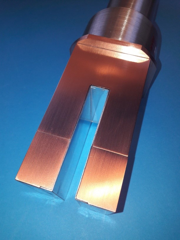
Detectors are usually manufactured in cylindrical housings made of e.g. plastics (only non-hygroscopic crystals), aluminum, stainless steel or (OHFC) copper. Square or rectangular housings add to the cost. Aluminum has excellent radiation transmission properties but is relatively soft and can corrode, even when anodized. For aggressive or rough environments (shocks), 316 type stainless steel is advised. Copper is useful for low background applications.
All detectors can be provided with customer defined mounting flanges or other means to support the instrument.
Light Pulsers
The light yield of a scintillation material and the gain of a light detector with amplification (e.g. PMT, SiPm) is a function of temperature. As discussed in earlier, it is possible to calibrate a scintillation detector on a light pulse emitted by e.g. a stabilized LED or by the light emitted by a radioactive pulser. This can be :
The advantage of method 1 is that one calibrates on the true response of the primary crystal. However, many gamma sources have more than one line and there is also Compton background.
The advantages of alpha sources is the absence of Compton background and their high energy (usually around 5 MeV) which implies narrow lines. The disadvantage is that the temperature response of many scintillation crystals is different for gammas and alphas. The optimum choice depends on the energy of interest and on the temperature region in which the detector should be stabilized.

LEDs are intrinsically unstable (temperature, ageing) and cannot be used for an absolute calibration of a scintillation detector without measuring the emitted light in another way ( e.g. with a diode).
Low Background Detectors
The term low background in itself needs to be specified in detail. A proper specification is the number of counts within a certain energy window with a well-defined shielding around the instrument (Pb, Fe and Cu).
Below a schematic shows the different sources of background in a shielded scintillation detector set-up.
Sources of background from within the detector are the photomultiplier tube or other light detector, the detector housing and the scintillator. The main contributing nuclides are 40K (mainly from the PMT glass) and U and Th which are present in small quantities in the housing and window materials. Special PMTs can be selected with a ultra-low K content and all other materials can be pretested prior to assembling. Plastics should be avoided because they often contain K. Aluminum has a larger U and Th content than steel so for low background applications, steel housings are the best choice.
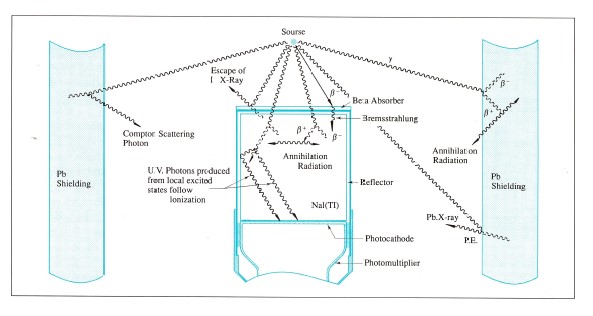
Sources of background from within the detector are the photomultiplier tube or other light detector, the detector housing and the scintillator. The main contributing nuclides are 40K (mainly from the PMT glass) and U and Th which are present in small quantities in the housing and window materials. Special PMTs can be selected with a ultra-low K content and all other materials can be pretested prior to assembling. Plastics should be avoided because they often contain K. Aluminum has a larger U and Th content than steel so for low background applications, steel housings are the best choice.
SiPms and photodiodes have little mass and are relatively background free.
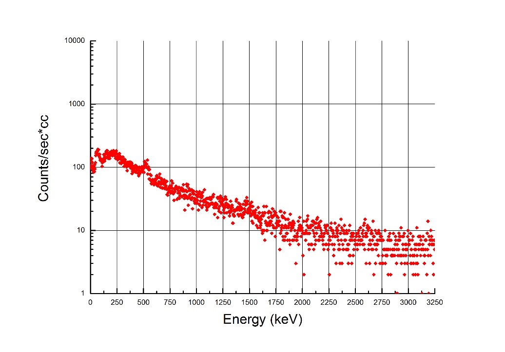
In low background detectors special precautions are taken to reduce the internal background. Between PMT and crystal quartz or undoped NaI light guides are used to absorb the beta radiation from 40K and to increase the distance between the PMT and the scintillation crystal. Below a typical NaI(Tl) background spectrum is shown. The continuum is caused by cosmic interactions (muons) in the scintillator and the shielding.
The scintillation crystal is a source of internal contamination too. NaI(Tl) crystals have a low background with their 40K content is less than 1 ppm.
Typical NaI(Tl) background spectrum in shielding
Other scintillators have typical radiological background issues. All CsI(Tl) crystals have some Cs-137 contamination due to nuclear fallout incidents over the last decades.
BGO crystals have an internal background caused by traces of 206Pb that are transmuted by cosmic radiation into 207Bi, resulting in gamma lines at 570, 1060, 1630 (sum peak) and 2400 keV. Typical net count rates in the above peaks are approx. 0.001 c/s/cc.
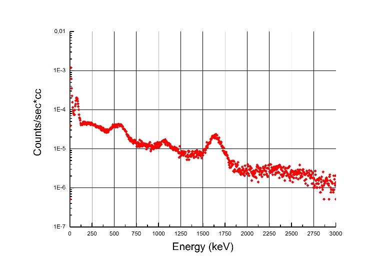
Typical BGO background spectrum in 10 cm thick Pb shielding
BaF2 crystals have an intrinsic background of Radium causing a set of alpha lines with a total count rate of 0.25 c/s/cc typical.
CeBr3 crystals have a typical Ac-227 background due to alpha particles of at best < 0.001 c / s / cc whereas SrI2(Eu) crystals are very radiopure. The best large volume scintillation crystal for very low background applications is still NaI(Tl).
This site uses cookies. By continuing to browse the site, you are agreeing to our use of cookies.
AgreeLearn moreWe may request cookies to be set on your device. We use cookies to let us know when you visit our websites, how you interact with us, to enrich your user experience, and to customize your relationship with our website.
Click on the different category headings to find out more. You can also change some of your preferences. Note that blocking some types of cookies may impact your experience on our websites and the services we are able to offer.
One button to accept all cookies and services with a single click.
These cookies are strictly necessary to provide you with services available through our website and to use some of its features.
Because these cookies are strictly necessary to deliver the website, you cannot refuse them without impacting how our site functions. You can block or delete them by changing your browser settings and force blocking all cookies on this website.
One button to accept all cookies and services with a single click.
Refuse cookies and hides message bar.
Opt out from all the cookies (except 2 from av_privacy_allow_cookies)
Disable Google tracking
Disable Google webfonts
Disable Google reCaptcha
Disable Google Maps
Disable video embeds
Adds an accept cookies button
Adds a do not accept cookies button
These cookies collect information that is used either in aggregate form to help us understand how our website is being used or how effective our marketing campaigns are, or to help us customize our website and application for you in order to enhance your experience.
If you do not want that we track your visist to our site you can disable tracking in your browser here:
We also use different external services like Google Webfonts, Google Maps and external Video providers. Since these providers may collect personal data like your IP address we allow you to block them here. Please be aware that this might heavily reduce the functionality and appearance of our site. Changes will take effect once you reload the page.
Google Webfont Settings:
Google Map Settings:
Vimeo and Youtube video embeds:
You can read about our cookies and privacy settings in detail on our Privacy Policy Page.